ABSTRACT
In the present paper electrical characteristics of Al/SiO2/p-Si MIS structure was measured in the range of voltage ±4V. Silicon layer SiO2 on the
semiconductor wafer was obtained by thermal oxidation of Si. The Al/SiO2/p-Si (MIS) structures were constructed on p-type (boron-doped) single-crystal silicon
wafers with a (100) surface orientation. The a thickness of wafer is 350 μm, a diameter of 2 inches, and a resistivity of 1 Ω.cm. The thickness of SiO2 layer in
the MIS structure is 60 nm. On the basis of measured characteristics have been obtained basic parameters of structure such as potential barrier heigt (ϕB0),
ideality –factor (n) and series-resistance (Rs). For the calculating of parameters have been used two methods - thermionic-emission (TE) theory and Cheung’s
functions. The results obtained by both methods were compared. The identified differences are due to the presence of inhomogeneities at the interface and in the volume.
Keywords: Schottky diode; Thermionic emission; Cheung’s functions; Surface state density, Metal- insulator- semiconductors (MIS); SiO2
DOI:10.70784/azip.3.2024CE91
Received: 2024
Internet publishing: 2024
AUTHORS & AFFILIATIONS
Baku State University, AZ1148, Baku, Azerbaijan
E-mail:
Graphics and Images
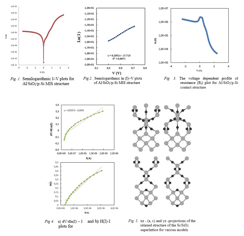
Fig.1-2-3-4-5
|
[1] S.M. Sze. Physics of Semiconductor Devices, second ed., Willey, New York, 1981.Roder.
[2] V.I. Strikha. Theoretical bases of metal–semiconductor contact’s work. Kiev: Naukova Dumka; 1974 [in Russian].
[3] E.H. Rhoderich. Metal–semiconductor contacts. Moscow: Radio I svyaz; 1982 [in Russian]. R. Castagne, A. Vapaille, Surface Science 28(1), 157 (1971).
[4] J.M. Poate, K.N. Tu, J.W. Mayer. Thin films – interdiffusion and reactions. Moskow: Mir; 1982 [in Russian].
[5] E.V. Buzanyova. Microstructures of integrated electronics. Moscow, Radio i Svyaz, 1990.
[6] U. Kelberlau, R. Kassing. Solid-State Electron. 24, 321 (1981).
[7] N. Konofaos, E.K., Evangelou, Zhongchun Wang, V. Kugler, U. Helmersson. Journal of Non Crystalline Solids. 303, 185 (2002).
[8] E.J. Miller, X.Z. Dang, H.H. Wieder, P.M. Asbeck, E.T. Yu, G.J. Sullivan, J.M. Redwing.J. Appl. Phys., 87(11), 8070 (2000).
[9] Ş. Altındal, H. Kanbur, İ.Yücedağ, A. Tataroğlu. Microelect. Eng. 85, 1495 (2008).
[10] A. Tataroğlu, Ş Altındal. Microelect. Eng.85, 2256 (2008).
[11] M. Kuhn. Solid State Electron. 13(6), 873 (1970).
[12] Ş. Altindal, Y. Şafak Asar, A. Kaya, Z. Sönmez. Investigation of interface states in Al/SiO2/p-Si (MIS) structures with 50 and 826 Å SiO2 interfacial layer using admittance spectroscopy method/Journ. of optoelectronics and advanced materials, vol. 14, № 11- 12, 2012, p. 998 – 1004.
[13] E.H. Nicollian, J.R. Brews. MOS (metal/oxide/semiconductor) Physics and Technology, John Wiley & Sons, New York (1982).
[14] A. Tataroğlu, Ş Altındal. Microelect. Eng. 85, 2256 (2008).
[15] W. Mönch. Semiconductor Surfaces and Interfaces, third ed. Springer Verlag Pres, 2001.
[16] M. Çakar, A. Türüt. Synthetic Metals, 13, 549 (2003).
[17] Y. Çağlar, M. Çağlar, S. Ilican, F. Yakuphanoğlu. Microelect. Eng., 86, 2072 (2009).
[18] L. Truong, Y. G. Fedorenko, V.V. Afanasev, A. Stesmans. Microelectronics Reliability, 45, 823 (2005).
[19] A. Tataroğlu. J. Optoelectron. Adv. Mater.13(8), 940 (2011).
[20] E.H. Nicollian, A. Goetzberger. Bell Syst.Tech. J. 46, 1055 (1967).
[21] K.K. Hung, Y.C. Cheng. Appl. Surf. Sci., 30, 114 (1987).
[22] E.H. Nicollian, A. Goetzberger, A.D. Lopez. Solid-State Electron. 12, 937 (1969).
[23] C.N. Berglund. IEEE Trans. Nucl. Sci. ED-13(10), 701 (1966).
[24] A. Tataroğlu, Ş. Altındal, M.M. Bülbül. Microelect. Eng. 81, 140 (2005).
[25] S.K. Cheung, N.W. Cheung. 1998. Extraction of Schottky diode parameters from forward current-voltage characteristics. Applied Physics Letters, 49, 85.
[26] Р.М.Х. Исхакзай, В.Н. Кручинин, В.Ш. Алиев, В.А. Гриценко, Е.В. Дементьева, М.В. Заморянская. Pанспорт заряда в нестехиометрическом SiOx, полученном обработкой термического SiO2 в водородной плазме электронно-циклотронного резонанса. Микроэлектроника, 2022, T. 51, № 1, стр. 28.
[27] С.С. Некрашевич, В.А. Гриценко. Электронная структура оксида кремния (Обзор) Физика твердого тела, 2014, том 56, вып. 2, с.209-223.
|