ABSTRACT
The main parameters of Re/n-GaAs Schottky barrier diodes (SBDs) were investigated at room temperature by the forward and reverse bias current–voltage (I–V), capacitance–
voltage (C–V) and conductance–voltage (C/ω-V).The diodes were fabricated by using PLD technique. Characteristics parameters such as potential barrier height (ΦB), ideality
factor (n) and series resistance (Rs) have been calculated by using different methods and compared. Furthermore, the voltage-dependent profile of the resistance (Ri) and
shunt resistance (Rsh) were obtained for Re/n-GaAs Schottky diodes from the I–V data using Ohm's law. In addition, the influence of frequency on parameters have been
investigated. From the reverse bias C-2 versus V plots the Fermi energy level EF, doping concentration ND and potential barrier height for each frequency have been
obtained. The dependence of parameters on frequency due to surface state have been revealed.
Keywords: Re/n-GaAs Schottky barrier diodes (SBDs); Frequency dependence; Series resistance; Surface states, Impedance spectroscopy;
DOI:10.70784/azip.1.2024337
Received: 01.10.2024
Internet publishing: 11.10.2024
AUTHORS & AFFILIATIONS
1. Baku State University, Baku, AZ1148, Azerbaijan
2. Department of Chemical Engineering, Faculty of Engineering, Gazi University, Ankara, Turkey
*Corresponding author: E-mail: I_afandiyeva@yahoo.com
Graphics and Images
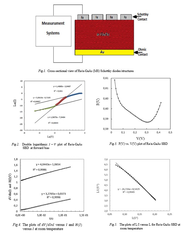

Fig.1-2-3-4-5 Fig.6-7-8
|
REFERENCIES
[1] E.H. Rhoderick, R.H. Williams. Metal–Semiconductor Contacts, Clarendon Press, Oxford, 1988.
[2] V.I. Strikha. Theoretical Bases of Metal-Semiconductor Contact Work, Naukova Dumka, Kiev, (1974) (in Russian).
[3] S.M. Sze. Physics of Semiconductor Devices, John Wiley & sons, New York, 1981.
[4] I.M. Afandiyeva, Ş. Altιndal, L.K. Abdullayeva, A.İ. Bayramova. Self-assembled patches in PtSi/n-Si (111) diodes, Journal of Semiconductors, 2018, v.39, n5, pp.054002-1-7.
[5] F. Taghizadeh, van Rensburg, P.J. Janse, K. Ostvar, et al. Electronic properties and transformation kinetics of two prominent metastable defects introduced in GaAs during sputter deposition of Au Schottky contacts/Materials science in semiconductor processing / 2019,v.99, pp.23-27.
[6] B. Kirezli, M. Ahmetoglu (Afrailov), A. Kara. Electrical and optical properties of photodiode structures formed by surface polymerization of [P (EGDMA-VPCA)-SWCNT] films on n-GaAs/Journal of molecular structure, 2019, vol.1192, pp. 258-263.
[7] Vezzoli, Andrea; Brooke, Richard J. Ferri, Nicolo et al. Charge transport at a molecular GaAs nanoscale junction/Faraday Dıscussıons, 2018, vol. 210, pp. 397-408.
[8] Chatterjee, Abhishek; K. Khamari, Shailesh ; S. Porwal. Effect of Co-60 gamma-irradiation on the nature of electronic transport in heavily doped n-type GaN based Schottky photodetector/, 2018, vol.123, is.16, 161585.
[9] B.S. Danilin. Vakuum evaporation of thin films,M.Energiya, 1967, 312p.
[10] Contelot, Fanny, Thomas, J. Robert, Seaman, John C. Using porous iron composite (PIC) material to immobilize rhenium as an analogue for technetium. Environment InternationaL, 2019, vol. 128, pp. 379-389.
[11] Littleton, A.H. Joshua Secco, A. Richard, Yong, Wenjun et.al. Electrical resistivity and thermal conductivity of W and Re up to 5 GPa and 2300 K/Journal of Applied Physics, 2019, 125, is.13, 135901.
[12] Tian, Bian; Yu, Qiuyue; Zhang, Zhongkai et.al. Effect of magnetron sputtering parameters on adhesion properties of tungsten-rhenium thin film thermocouples Ceramics International, 2018, vol.4 p15-18.
[13] Hasanli, Nijat; Gauquelin, Nicolas; Verbeeck, Johan. Small-moment paramagnetism and extensive twinning in the topochemically reduced phase Sr2ReLiO5.5 Dalton Transactions, 2018, vol.47, is.44, pp.15783-15790.
[14] Chia-Chien Lin. Electrical and structural properties of Re/GaAs Schottky diodes/Journal of Applied Physics 85, 3893, 1999.
[15] Durmus, H Yildirim, M., Altindal, S .On the possible conduction mechanisms in Rhenium/n-GaAs Schottky barrier diodes fabricated by pulsed laser deposition in temperature range of 60-400K/ journal of materıals scıence-materıals ın electronıcs/ 2019, vol. 30, is.9, pp. 9029-9037.
[16] Ya.Ya. Kudryk, V.V. Shynkarenko, V.S. Slipokurov et al. /Determination of the Schottky barrier height in diodes based on Au–TiB2–n-SiC6H from the current-voltage and capacitance-voltage characteristics/ Semiconductor Physics, Quantum Electronics & Optoelectronics, 2014. V. 17, № 4. P. 398-402.
[17] S.O. Tan, H. Uslu, O.C. Tecimer. Electrical characterizations of Au/ZnO/n-GaAs Schottky diodes under distinct illumination intensities/J Mater Sci: Mater Electron. 2016, DOI 10.1007/s10854-016-4843-4.
[18] Abdulkerim Karabulut. Barrier height modification in Au/Ti/n-GaAs devices with a HfO2 interfacial layer formed by atomic layer deposition/ Bull. Mater. Sci. (2019) 42:5.
[19] K. Bouzidi, M. Chegaar, M. Aillerie. Solar cells parameters evaluation from dark I-V Characteristics/ Energy Procedia 18 (2012) 1601 – 1610.
[20] H. Norde. A modified forward I-V plot for Schottky diodes with high series resistance, J. Appl. Phys.1979:50;5052-5053S.
[21] S.K. Cheung, N.W. Cheung. Extraction of Schottky diode parameters from forward current-voltage characteristics. Appl. Phys. Lett. 49(2), p. 85-87. (1986).
[22] J.H. Werner. Schottky barrier and pn-junction I/V plots -Small signal evaluation, Appl Phys A, 1988, 47:291-300.
[23] N. Şimşir, H. Şafak, ÖF Yüksel, M. Kuş. Investigation of current–voltage and capacitance–voltage characteristics of Ag/perylene-monoimide/GaAs Schottky diode. Curr Appl Phys 2012; 12: 1510-1514.
[24] I.M. Afandiyeva, R.F Babayeva. The potential barrier height and profile of surface states of Re/n-GaAs Schottky barrier diode, Proc. of the 7th Int. Conf. MTP-2021: Modern Trends in Physics, dec. 15-17, 2021, BSU, Baku, Azerbaijan, pp.97-103.
[25] A. Kaya, E.Marıl, Ş. Altındal, İ. Uslu. The comparative electrical characteristics of Au/n-Si (MS) diodes with and without a 2% graphene cobalt-doped Ca3Co4Ga0.001Ox interfacial layer at room temperature/Microelectronic Engineering 149 (2016) 166–171.
[26] P.N. Krylov. Physical models of thermo-processed contact metal–semiconductors. Journal of Udmurt University, 2006, 4: 125.
[27] M P. Shaskolskaya.Crystallography. Moscow, Visshaya shkola, 1984.
[28] C. Calandra, Giorgio Santoro. Surface states of the (110) surface of GaAs,Journal of Physics C Solid State Physics 8(6):L86. 2001.
[29] Erman Erdoğana, MutluKundakçıb Room temperature current-voltage (I-V) characteristics of Ag/InGaN/n-Si Schottky barrier diode/ Physica B: Condensed Matter,Volume 506, 1 February 2017, Pages 105-108.
[30] Haziret Durmuş and Ülfet Atav. Extraction of voltage-dependent series resistance from I-V characteristics of Schottky diodes/ Appl. Phys. Lett. 99, 093505 (2011).
[31] O.A. Soltanovich, N.M. Shmidt, E.B. Yakimov. Frequency and temperature dependences of capacitance–voltage characteristics of InGaN/GaN light-emitting structures with multiple quantum wells. Semiconductors, 2011, 45(2): 221.
[32] S.J. Moloi, M. McPherso. Capacitance–voltage behaviour of Schottky diodes fabricated on p-type silicon for radiation-hard detectors. Radiation Physics and chemistry, 2013, 85:73.
[33] I.S. Yahiya, H.Y. Zahran, F.H. Alamri, M. Aslam. Microelectronic properties of the organic Schottky diode with pyronin-Y: Admittance spectroscopy, and negative capacitance. Physica B: Condensed Matter, 2018, 543: 46.
[34] G. Ersöz, I. Yücedağ, Y. Azizian-Kalandaragh, I. Orak, S. Altındal. Investigation of Electrical Characteristics in Al/CdS-PVA/p-Si (MPS) Structures Using Impedance Spectroscopy Method/ IEEE transactıons on electron devıces, v. 63, № 7, July 2016, p.2948-2955.
[35] F. Parlakturk, S. Altındal, A. Tataroğlu, M. Parlak, A. Agasiev. On the profile of frequency dependent series resistance and surface states in Au/Bi4Ti3O12/SiO2/n-Si(MFIS) structures, p.81-88.
[36] E.H. Nicollian and J.R. Brews. MOS (Metal Oxide Semiconductor) Physics and Technology. New York, USA: Wiley, 1982, pp. 117–129.
|