ABSTRACT
In this study, we investigate the electrical properties of a Au/7%Ni-doped PVP/n-Si metal–polymer–semiconductor (MPS) structure. The study focuses on the influence of the
Ni-doped interfacial polymer layer on the device’s low-frequency behavior. Electrical characterization was carried out using capacitance–voltage (C–V), conductance over
angular frequency–voltage (G/ω–V), and series resistance–voltage (Rs–V) measurements. All measurements were performed at room temperature (300 K), in the voltage range
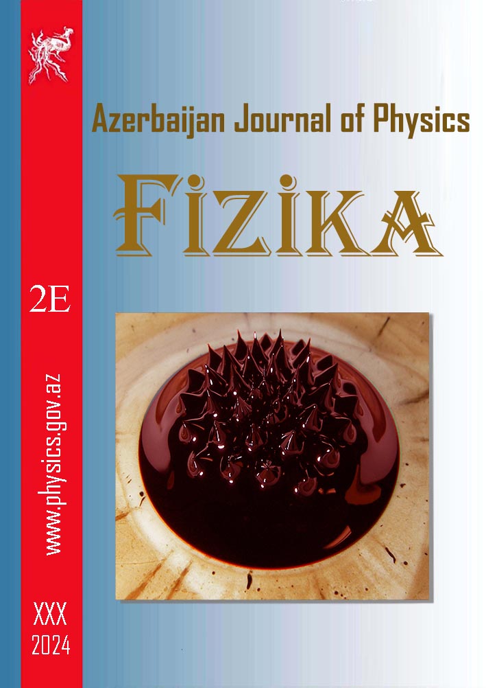
from –4.5 V to +3.5 V, using two low-frequency conditions: 100 Hz and 200 Hz. A pronounced frequency-dependent dispersion was observed in both C–V and G/ω–V characteristics,
particularly near +1.2 V, indicating strong interfacial polarization and trap-related effects. The peak capacitance at 100 Hz reached approximately 9.4 × 10⁻¹⁰ F, decreasing
at higher frequency due to the reduced response of surface states. Series resistance, extracted using the Nicollian–Brews method, showed significant variation with both
voltage and frequency, confirming the active role of interfacial traps and dipolar relaxation in the Ni-doped PVP layer. These findings demonstrate that Ni incorporation
substantially modifies the dielectric and resistive properties of the interface, enhancing the sensitivity of the device to frequency-dependent surface state dynamics.
Keywords: Metal–Polymer–Semiconductor (MPS), Ni-doped PVP, Schottky diode, Capacitance–Voltage (C–V), Conductance–Voltage (G/ω–V), impedance spectroscopy, Interface states.
DOI:10.70784/azip.1.2026132
Received: 16.02.2026
Internet publishing: 19.02.2026 AJP Fizika E 2026 1 en p.32-37
AUTHORS & AFFILIATIONS
Baku State University, Department of Physics, Baku,Azerbaijan
E-mail: elvinb18104@sabah.edu.az, I_afandiyeva@yahoo.com
Graphics and Images
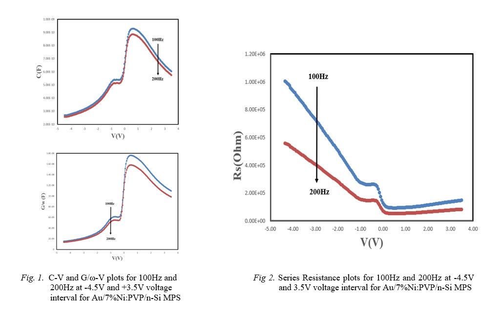
Fig.1-2
|
[1] N.A. Al-Ahmadi. Metal oxide semiconductor-based Schottky diodes: a review of recent advances. Materials Research Express, 7 (2020) 03200; https://doi.org/10.1088/20531591/ab7a60.
[2] N. Balaram, M. Siva Pratap Reddy, V. Rajagopal Reddy, C. Park. Effects of high-k zirconium oxide (ZrO₂) interlayer on the electrical and transport properties of Au/n-type InP Schottky diode. Thin Solid Films, 619 (2016) 231–238; https://doi.org/10.1016/j.tsf.2016.10.060.
[3] S.M. Sze, K.Ng Kwok. Physics of Semiconductor Devices. (New Jersey: John Wiley & Sons, 2007).
[4] E.H. Nicollian, J.R. Brews. MOS (Metal Oxide Semiconductor) Physics and Technology. (New Jersey: John Wiley & Sons, 2002).
[5] S. Demirezen, Ş. Altındal, Y. Azizian-Kalandaragh, A. M. Akbaş. A comparison of Au/n-Si Schottky diodes (SDs) with/without a nanographite (NG) interfacial layer by considering interlayer, surface states (Nss) and series resistance (Rs) effects. Phys. Scr., 97 (2022) 055811; https://doi.org/10.1088/1402-4896/ac645f.
[6] A. Khalkhali, E. Erbilen Tanrıkulu, S. Altındal Yerişkin, A. Arslan Alsaç, K. Yıldız. A study regarding dielectric response and ac electrical conductivity of Schottky structures (SSs) interlaid with (Fe2O3-PVA) by using dielectric spectroscopy method. J. Inorg. Organomet. Polym., (2025); https://doi.org/10.1007/s10904-025-03667-x.
[7] B. Akın, S. A. Hameed, S. Altındal Yerişkin, M. Ulusoy, H. Durmuş. The probe of current conduction mechanisms, interface states, and the forward bias intersection point of the Al/Al2O3/Ge/p-Si heterostructures depending on temperature. Materials Science in Semiconductor Processing, 184 (2024) 108781; https://doi.org/10.1016/j.mssp.2024.108781.
[8] İ. Taşçıoğlu, G. Pirgholi-Givi, S. Altındal Yerişkin, Y. Azizian-Kalandaragh. Examination on the current conduction mechanisms of Au/n-Si diodes with ZnO-PVP and ZnO/Ag2WO4-PVP interfacial layers. J. Sol-Gel Sci. Technol., 107 (2023) 536–547; https://doi.org/10.1007/s10971-023-06177-9.
[9] H.G. Çetinkaya, A. Feizollahi Vahid, N. Basman, S. Demirezen, Y. Şafak Asar, S. Altındal. On the wide range frequency and voltage dependence of electrical features and density of surface states of the Al/(Cu:DLC)/p-Si/Au Schottky diodes (SDs). J. Mater. Sci.: Mater. Electron., 34 (2023) 822; https://doi.org/10.1007/s10854-023-10247-7.
[10] A.E. Tezcan, S.A. Hameed, A.F. Vahid, M. Ulusoy, Ş. Altındal. A study on the complex dielectric (ε*)/electric-modulus (M*)/impedance (Z*), tangent-loss(tanδ), and ac conductivity (σac) of the Al/(S:DLC)/p-Si/Au (MIS)-type Schottky structures in a wide range of frequency and voltage at room temperature (RT). Physica B: Condensed Matter, 684 (2024) 415959; https://doi.org/10.1016/j.physb.2024.415959.
[11] Ç.Ş. Güçlü, M. Ulusoy, Ş. Altındal. A comparison electrical characteristics of the Au/(pure-PVA)/n-Si and Au/(CdTe doped-PVA)/n-Si (MPS) type Schottky structures using I-V and C-V measurements. J Mater Sci: Mater Electron, 35 (2024) 881; https://doi.org/10.1007/s10854-024-12650-0.
[12] A.A. Alarabi, O. Çiçek, H. Makara, F. Ünal, M. Zurnacı, Ş. Altındal. Enhanced sensing capabilities of UV-visible p-n and p-i-n photodiodes using unique layer and contact configurations. Engineering Science and Technology, an International Journal, 62 (2025) 101975; https://doi.org/10.1016/j.jestch.2025.101975.
[13] A.S. Dinçer, M.T. Haliloğlu, A. Toprak, Ş. Altındal, E. Özbay. Effect of Si-rich SiXNY multilayer passivation material on the DC electrical characteristics of AlGaN/GaN HEMTs. J Mater Sci: Mater Electron, 34 (2023) 1674; https://doi.org/10.1007/s10854-023-11077-3.
[14] O. Çiçek, E. Arslan, Ş. Altındal, Y. Badali, E. Özbay. 21.2 mV/K High-Performance Ni(50 nm)-Au(100 nm)/Ga2O3/p-Si Vertical MOS Type Diode and the Temperature Sensing Characteristics With a Novel Drive Mode. IEEE Sensors Journal, 22 (2022) 23699–23704; https://doi.org/10.1109/JSEN.2022.3219553.
[15] D. Yılmaz, O. Odabaşı, G. Salkım, E. Urfali, B. Çankaya Akoğlu, E. Özbay, Ş. Altındal. DC and RF performance of lateral AlGaN/GaN FinFET with ultrathin gate dielectric. Semiconductor Science and Technology, 37 (2022) 085008; https://doi.org/10.1088/1361-6641/ac7818.
[16] A. Chelkowski. Dielectric Physics. Elsevier, Amsterdam, 1980.
[17] G. Kandhol, H. Wadhwa, S. Chand, S. Mahendia, S. Kumar. Study of dielectric relaxation behavior of composites of Poly (vinylalchohol) (PVA) and Reduced graphene oxide (RGO). Vacuum, 160 (2019) 384–393; https://doi.org/10.1016/j.vacuum.2018.11.051.
[18] M. Sharma, S. K. Tripathi, Frequency and voltage dependence of admittance characteristics of Al/Al2O3/PVA:n-ZnSe Schottky barrier diodes. Materials Science in Semiconductor Processing, 41 (2016) 155–161; https://doi.org/10.1016/j.mssp.2015.07.028.
[19] O.G. Abdullah, Y.A. Salman, S.A. Saleem. Electrical conductivity and dielectric characteristics of in situ prepared PVA/HgS nanocomposite films, J Mater Sci: Mater Electron, 27 (2016) 3591–3598; https://doi.org/10.1007/s10854-015-4196-4.
[20] Y. Badali. Electrical properties of (PVC:BN) nanocomposite as interfacial layer in metal semiconductor structure. J Mater Sci: Mater Electron, 35 (2024) 513; https://doi.org/10.1007/s10854-024-12253-9.
[21] A. Ashery, S. A. Gad, H. Shaban. Frequency and temperature dependence of dielectric properties and capacitance–voltage in GO/TiO2/n-Si MOS device, Appl. Phys. A 126 (2020); https://doi.org/10.1007/s00339-020-03729-6.
[22] G.C. Psarras. Fundamentals of dielectric theories, in: Dielectric Polymer Materials for High-Density Energy Storage, Elsevier, 2018, pp. 11–57; https://doi.org/10.1016/B978-0-12-813215-9.00002-6.
[23] M. Gökçen, T. Tunç, Ş. Altındal, İ. Uslu. Electrical and photocurrent characteristics of Au/PVA (Co-doped)/n-Si photoconductive diodes, Mater. Sci. Eng. B 177 (2012) 416–420; https://doi.org/10.1016/j.mseb.2012.01.004.
[24] Ç. Bilkan, Y. Azizian-Kalandaragh, Ş. Altındal, R. Shokrani-Havigh. Frequency and voltage dependence dielectric properties, ac electrical conductivity and electric modulus profiles in Al/Co₃O₄-PVA/p-Si structures, Physica B 500 (2016) 154–160; https://doi.org/10.1016/j.physb.2016.08.001.
[25] B.K. Jones, J. Santana, and M. McPherson. Negative capacitance effects in semiconductor diodes, Solid State Commun. 107(1988) 47; https://doi.org/10.1016/S0038-1098(98)00162-8.
[26] S. Bengi, H.G. Çetinkaya, Ş. Altındal, S. Zeyrek. Examination of Electrical and Dielectric Parameters of Au/n Si Schottky Barrier Diodes (SBDs) with Organic Perylene Interlayer Using Impedance Measurements Under Various Illumination Intensities, J. Electron. Mater. 53 (2024) 5606–5616; https://doi.org/10.1007/s11664-024-11213-7.
[27] S.A. Butcher, T.L. Tansley, D. Alexiev. An instrumental solution to the phenomenon of negative capacitances in semiconductors, Solid-State Electronics 39, 333–336 (1996); https://doi.org/10.1016/0038-1101(95)00143-3.
[28] X.L. Huang, Y.G. Shin, K.Y. Lim, E.-K. Suh, H.J. Lee, S.C. Shen. Thermally induced capacitance and electric field domains in GaAsAl0.3Ga0.7As quantum well infrared photodetector, Solid-State Electronics 41, 6 (1997); https://doi.org/10.1016/S0038-1101(97)00027-0.
[29] M. Ershov, H. C. Liu, L. Li, M. Buchanan, Z.R. Wasilewski, and A.K. Jonscher, Negative capacitance effect in semiconductor devices, IEEE Trans. Electron Devices 45, 10 (1998) 2196–2206; https://doi.org/10.1109/16.725254
[30] A. Abidinov, I. Afandiyeva, E. Bakhtiyarli, S. Altındal Yerişkin, S.A. Hameed. Comprehensive Investigation of Negative Capacitance and Inductive Behavior in Pure and 3% and 5% Ni-Doped PVP-Based Au/n-Si (MS) Schottky Diodes (SDs), ACS Applied Electronic Materials 7 (20) (2025) 9399–9407, https://doi.org/10.1021/acsaelm.5c01377
[31] I.M. Afandiyeva, E.R. Bakhtiyarli, S. Altındal Yerişkin, S.A. Hameed. Negative dielectric and inductive behavior in Au/n-Si diodes with Ni-doped PVP interlayers, Journal of Materials Science: Materials in Electronics (2026), https://doi.org/10.1007/s10854-026-16574-9
[32] A.S. Abdinov, I.M. Afandiyeva, E.R. Bakhtiyarli. Electrical properties and dual barrier phenomena in Au/3% and 5% Ni-doped PVP/n-Si Schottky diodes : role of interlayer engineering, AJP FIZIKA 2025 volume XXXI № 3, section:E, p.23-26.
|